
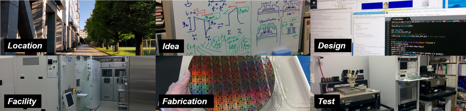
Our laboratory's motivations
~Creation of integrated technology by innovative nano-device for AI & IoT~
In today's highly information-oriented society, high-end servers are supporting IT infrastructures, and smart phones and sensor devices enable valuable services which make our life much more comfortable. The core of these electronic systems and devices is made by highly integrated semiconductor circuits. An integrated circuit consists of billions of silicon transistors and memory devices which are fabricated on a silicon wafer. Current transistor size is surprisingly reaching about 10nm or less. Internet-of-things (IoT) and Artificial Intelligence (AI) applications require new innovative transistor and memory device technologies. For the integrated circuit and system to be able to provide new deliverable values, we are exploring new innovative nanoelectronic devices.
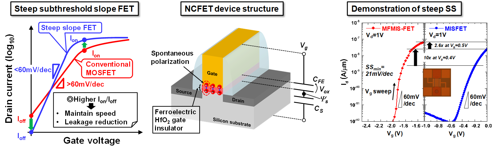
(1) Next generation transistor by new operation principle and structure
To realize an ultralow power circuit, the most effective way is to lower the supply voltage to the silicon transistors. However, transistor speed is at the cost when just reducing supply voltage. In order to solve this trade-off, the transistor has to turn on at lower gate voltage. The subthreshold slope of transistor is physically limited to 60mV/dec by thermal statistical mechanics at room temperature. There is a potential solution to overcome this physical limit: a negative capacitance transistor [5]. Negative Capacitance transistor (NCFET) has ferroelectric thin film as a gate insulator and its negative capacitance effectively amplifies transistor's channel potential and enables steep turn-on. We are investigating device physics of NCFET [2,4,6,7], proposing device design guideline for ultralow voltage operation [1,3], fabricating and demonstrating steep slope behavior and clarify its physical mechanism.
Reference: [1] M. Kobayashi et al., VLSI symposium (2015), [2] M. Kobayashi et al., IEDM (2016), [3] M. Kobayashi et al., IEEE Transactions on Nanotechnology (2017), [4] C. Jin et al., IEDM (2018), [5] M. Kobayashi, Applied Physics Express (Review) (2018), [6] C. Jin et al., VLSI Symposium (2019), [7] C. Jin et al., IEEE Transactions on Electron Devices (2020).
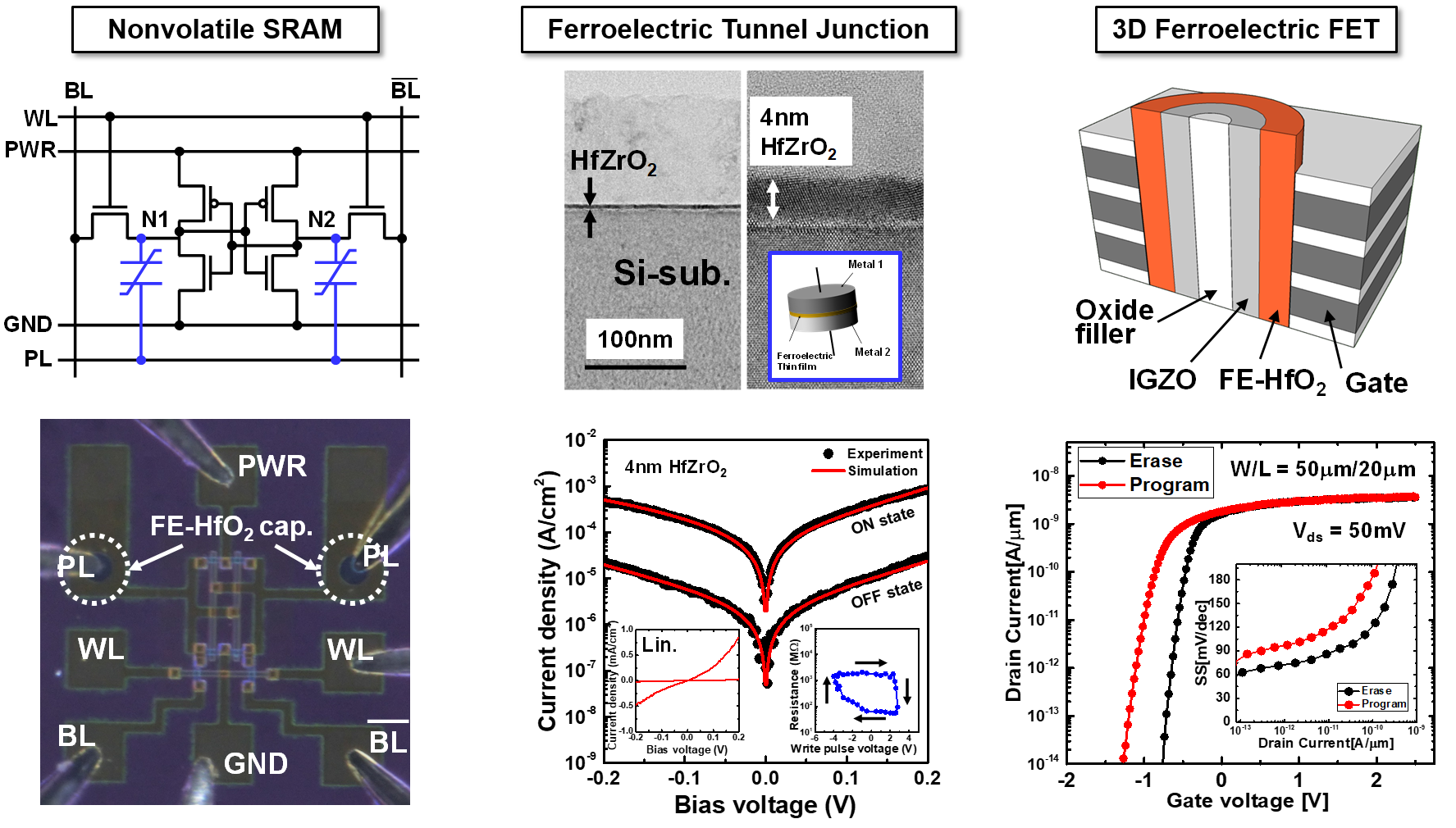
(2) High-capacity and low-power memory device using next generation ferroelectric material
It is inevitable to make full use of big-data in the data-driven society. However, available data sent from IoT edge device is much larger than the data traffic in cloud system, and thus it is challenging to fully utilize big-data. Then IoT edge device is expected to have large storage memory, run machine-learning algorithm and send only abstract data to cloud system. Since IoT edge device has limited power supply, such high-capacity memory needs to be lower-power. We are researching ferroelectric-HfO2 memory device, which is highly compatible with semiconductor integration process. Our research includes understanding of physical mechanism of ferroelectricity in HfO2 [5], smart power management technology by nonvolatile SRAM which consists of standard SRAM and ferroelectric-HfO2 capacitor [1], design and demonstration of ferroelectric tunnel junction (FTJ) memory for ultrahigh-density memory [2,3], 3D vertical FeFET with new channel material and operation principle [4,6].
Reference: [1] M. Kobayashi et al., VLSI Symposium (2017), [2] F. Mo et al., IEDM (2018), [3] M. Kobayashi et al., IEEE Journal of Electron Devices Society (2019), [4] F. Mo et al., VLSI Symposium (2019), [5] J. Wu et al., Applied Physics Letter (2020), [6] F. Mo et al., VLSI Symposium (2021, to be presented).
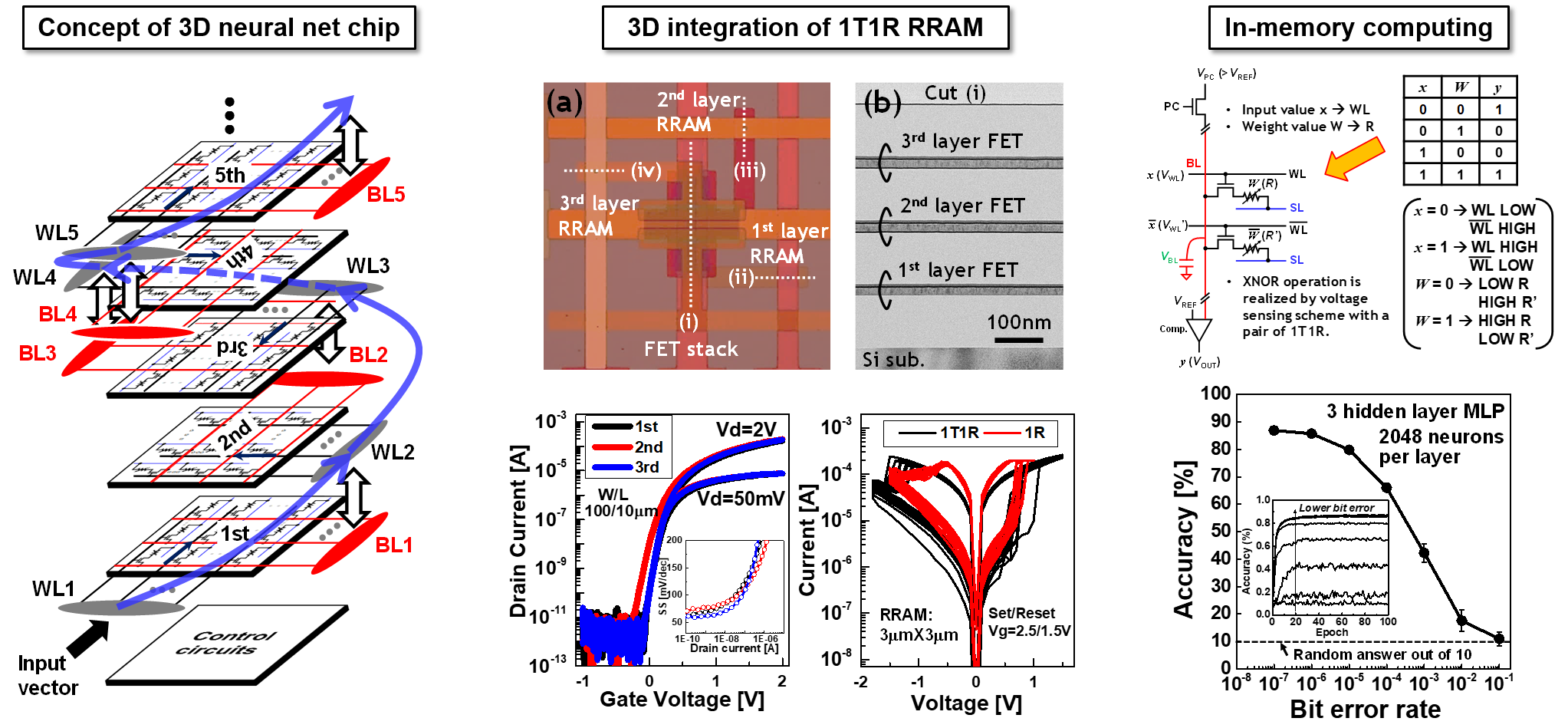
(3) Neuromorphic computing by novel 3D integration of oxide semiconductor FET and nonvolatile memory
Machine learning such as Deep learning is a source of innovation these days. Such algorithm is currently implemented by software on powerful CPU and GPU. Although software implementation is easy, very large power consumption is a serious issue. Especially, as described in (1), if we want to run machine-learning in IoT edge device, more energy-efficient computer architecture is necessary. Recently, neuromorphic computing, which mimics brain’s computing mechanism, has attracted attentions. Artificial neural network is an example of neuromorphic computing. By implementing neuron and synapse by using memory array and dedicated circuit, fundamental calculation of vector data and matrix data can be run in massive parallel manner. Usually such neural network is implemented in 2D array, however, we are exploring technology to implement neural network by 3D integration of oxide semiconductor FET and nonvolatile memory such as FTJ described in (2). This way, the 3D neural network can efficiently transfer and deliver data, which leads to energy-efficient computing.
Reference: [1] J. Wu et al., VLSI Symposium (2020), [2] J. Wu et al., VLSI Symposium (2021, to be presented).
Previous researches are here